

In the ever evolving industry of electronics manufacturing, producing efficient and cost-effective PCBs is paramount. This blog post aims to guide both purchasers and product designers to navigate the pitfalls of impractical and costly design and provide essential PCB design for manufacturing guidelines. By adhering to these principles, the production process can be optimised, product reliability bolstered and value for manufacturers and end-users maximised.
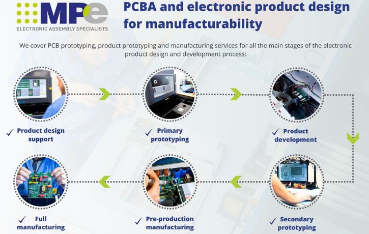
See how MPE supports PCB design for manufacturing services.
What is ‘design for manufacturing PCBs’
Design for Manufacturing (DFM) involves addressing any potential issues before a product is assembled. The PCB DFM process unites designers, product developers and chosen manufacturers into a collaborative team. Together, they scrutinise materials, environmental factors, layout and more to create a cost-effective and flawless design ready for production. This process identifies and rectifies potential design flaws through iterative improvements. Additionally, input from purchasers, vendors and legal experts can ensure seamless and efficient manufacturing without delays. In essence, PCB DFM illuminates what works and what doesn’t, paving the way for successful PCB production.
Why include PCB design for manufacturing in your assembly process?
Incorporating PCB design for manufacturing into the assembly process offers several advantages for product designers and purchasers:
- Streamlining the entire design, development and manufacturing process fosters better communication among all stakeholders.
- Cost savings are achieved by reducing manufacturing expenses, minimising delays and limiting excessive design iterations.
- Enhancing customer satisfaction by delivering reliable and fully functional end-products.
- Identifying opportunities to boost manufacturing efficiency.
- Upgrading existing or outdated designs for improved performance.
- Ensuring compliance with quality and safety standards, thereby enhancing product reliability and safety.
What are the key steps involved in the PCB DFM process?
The PCB DFM process encompasses the following essential areas to evaluate the suitability of the overall PCB design:
PCB layout design analysis: Pre-production analysis of the PCB’s layout, including trace width, components placement, clearance and spacing, thermal management, layer stack-up ensures alignment with its intended functionality.
Materials selection: Deliberation on product shape, size and application guides the selection of suitable materials, considering qualities such as thermal conductivity, dielectric constant (the material’s electrical insulation and polarisation properties), as well as overall strength, durability and texture.
Application considerations: Examination of the product’s anticipated application and environmental conditions, such as temperature, humidity, vibration etc.). Additionally, considerations for ease of maintenance and repair post-manufacture are assessed.
Manufacturing process selection: Collaboratively, designers, developers and manufacturers determine the most efficient manufacturing process based on factors such as design complexity, production volume, product size, material availability and the manufacturer/assembly partner’s in-house capabilities.
Testing and regulatory compliance: The PCB design undergoes scrutiny to ensure compliance with safety and quality regulations at local, national and international levels. Test points, test pads and built-in test features facilitate testing and troubleshooting. Third-party ISO certification bodies and impartial testing agents may assist with this step.
What are some common pitfalls of PCB design for manufacturing?
There are a number of potential design errors as well as process errors involved when it comes to PCB design. In this section, we delve into the most prevalent pitfalls:
Overly complex layout design
Overly complex PCB designs can increase manufacturing time and costs. Simplifying the design, reducing the number of layers and optimising component placement can improve manufacturability and reduce fabrication and assembly complexities.
Absence of sufficient solder masking between pads
A solder mask is a protective layer applied to the surface of a PCB to insulate copper traces (conductive pathways connecting electronic components) and pads (copper nodules on PCBs serving as component connection points) from environmental factors and unintended soldering during assembly. Omitting the solder mask between closely placed pads can result in solder bridging (i.e. where the adjacent copper traces come into contact with the pads), leading to short circuits. Special soldering techniques – if the chosen manufacturer/assembly partner has them at their disposal – are needed to prevent unwanted spread, which can potentially cause defects and rework.
Including vias in the PCB design
Although vias (plated holes that connect two or more conductive layers) play a role in freeing up space on PCBs, they can lead to ‘solder wicking’, which refers to drawing the solder away from the pads, thereby weakening the solder joint on the pad. Again, specialised manufacturing techniques may be required to ensure the integrity and reliability of vias in pads.
Inadequate Testability
Failing to include test points, fiducial marks (also known as reference marks) and other features for testing and inspection in the PCB design for manufacturability can hinder quality control and troubleshooting efforts during manufacturing.
Assumption of supported manufacturing processes
If PCB designers incorporate manufacturing processes not supported by their assembly partner, it can lead to compatibility issues and delays in production. It’s crucial for designers to select processes that align with their manufacturing partner’s capabilities and expertise.
PCB design for manufacturing guidelines – how to avoid mistakes and optimise efficiency
Having outlined common challenges in PCB DFM, we can now present PCB design for manufacturing guidelines to address such issues effectively:
Cutting costs
It is possible to reduce manufacturing costs as part of the DFM process by:
Reducing PCB size and layer count: Minimising the size and layer count of the PCB wherever possible decreases material costs and manufacturing complexity. Consolidating functionality and components reduces the overall footprint of the PCB without compromising performance.
Minimising drill and routing complexity: Simplifying the PCB layout minimises the number of drilled holes and routing complexity. Reducing the number of/removing vias from the design, using standard hole sizes, and avoiding intricate routing patterns lowers manufacturing costs associated with drilling and routing processes.
Using standardised components: Selecting off-the-shelf, standardised components whenever possible reduces component costs and lead times. Avoiding the inclusion of custom or proprietary components that require special manufacturing processes cuts costs.
Optimising material selection: Choosing cost-effective materials that meet the performance and reliability requirements of the PCB design. Selecting materials with lower material costs, such as standard laminate substrates and copper weights, while still ensuring adequate performance and durability.
Standardising PCB design for multiple applications: Designing PCBs for use in numerous products in order to reduce the production cost per unit and reduce overall testing costs.
Streamlining assembly processes: Designing for ease of assembly by minimising the number of components, optimising component placement and reducing assembly time and labour costs. Using surface-mount technology (SMT) components and automated assembly techniques to increase production efficiency and lower labour expenses.
Including design rules
Familiarising yourself with your chosen contract manufacturer or assembly partner’s capabilities is crucial for effective and efficient PCB production. Once you grasp these capabilities, you can integrate automated design rule checks to account for potential limitations, such as:
Component placement and number:
If the manufacturer has limitations on component sizes, types or number of placements per pass by their pick-and-place machines, design rules may specify component packages that are within the manufacturer’s capabilities.
Signal routing:
Design rules for trace width and spacing may be adjusted based on the manufacturer’s minimum feature sizes and tolerances for etching or milling.
Power distribution:
The manufacturer’s ability to achieve consistent copper thickness and layer registration during manufacture may determine the design rules for power plane clearance (spaces between
conductive layers carrying electrical power).
Material selection:
Design rules may specify laminate materials that are readily available from the manufacturer’s suppliers and are compatible with their manufacturing processes. Surface finish options, including coatings, may also be limited to those supported by the manufacturer’s facilities and expertise.
Detailed documentation
While the primary goal of PCB design for manufacturing is to minimise miscommunication between designers and manufacturers, errors can still occur despite longstanding partnerships. To mitigate these risks, sharing detailed documentation with your contract manufacturer or assembly partner is essential for early identification of design issues. This documentation typically includes:
- Gerber files: Standard format conveying PCB layout information to manufacturers.
- Bill of Materials (BOM): a comprehensive list of components and other materials required to produce your PCB assembly
- NC drill file: Standard format detailing hole locations and sizes on the PCB.
- Pick and place files: Offer component position, orientation, and identification for accurate assembly.
- Stack up: Defines layer arrangement and configuration.
- 3D files (where available): Represent physical characteristics for visualisation and analysis.
- Specified assembly instructions and preferred methods, as appropriate.
By providing comprehensive documentation, designers and manufacturers can ensure a smoother collaboration, minimise errors, and enhance the overall efficiency of the PCB manufacturing process.
Designed for maximum manufacturability with optimal yield
The overarching aim of the PCB design for manufacturing guidelines outlined above is to streamline the manufacturing process by ensuring that the final iteration of the PCB design can be seamlessly translated into a physical product with optimal efficiency and cost-effectiveness. By adhering to these guidelines, manufacturers can maximise the yield of high-quality PCBs, minimising production errors, reducing costs, and ultimately enhancing overall productivity and profitability.
Here at MPE, we offer PCB design as part of our expert PCB assembly and box build assembly service. Find out more here
MPE Electronics is an established and experienced contract electronics manufacturer specialising in PCB assemblies and full box build assembly for a wide range of commercial and industrial businesses.
To find out how MPE Electronics’ PCB manufacturing and assembly services can benefit your business, contact our expert and friendly team on +44 (0)1825 764822 or enquiries@mpe-electronics.co.uk.
