

As electronic products become smaller and more complex, multilayer PCBs are increasingly used to meet design and performance demands. Understanding how multilayer PCBs are made helps engineers, product developers and technical buyers to assess design trade-offs, identify manufacturing constraints and make better-informed decisions during development.
This guide explains how multilayer PCBs are made, where they’re used and what distinguishes them from simpler board types, as well as when a multilayer design is necessary.
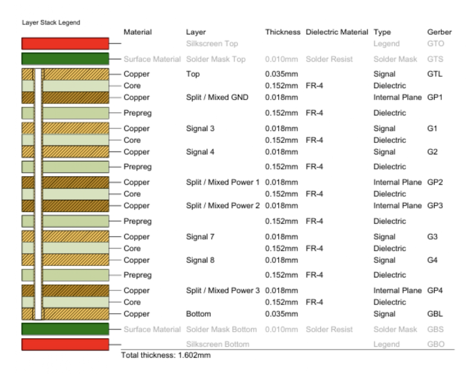
See how we support complex multilayer PCB builds
What Are Multilayer PCBs?
A multilayer PCB contains more than two layers of a conductive material such as copper, laminated and bonded together with heat-resistant insulating layers in between. These inner and outer layers are aligned and pressed under high temperature and pressure to form a single, solid structure.
While single layer PCBs have one conductive layer and double layer PCBs have two (one on each side of the substrate), multilayer PCBs use a stack-up of alternating conductors and insulators to support more complex routing and greater functionality.
How Do They Differ From Other PCBs?
Multilayer PCBs allow for denser circuit designs and smaller footprints. Unlike single or double-sided boards, they offer more internal layers to route connections. This makes it easier to handle fast signals, reduce electromagnetic interference (EMI) and keep power and data paths separate, which improves overall stability.
They are particularly suited to devices where space is limited and performance requirements are high. Examples include industrial controls, medical equipment and communications hardware.
How Are Multilayer PCBs Made?
Multilayer PCB manufacturing involves combining multiple conductive layers, typically copper, into a single, compact board through a controlled lamination process. Each step must maintain tight tolerances to ensure electrical integrity, mechanical stability and long-term reliability.
Step 1. Inner Layer Preparation
Each conductive layer starts with a copper-clad laminate. A photoresist layer (a light-sensitive polymer) is applied and then exposed to UV light through a photomask that defines the circuit pattern. The exposed areas harden, while the unexposed areas remain soft and are removed using a developer solution. This exposes the copper underneath.
Optical targets, also known as registration marks, are added to assist with alignment during lamination. Accurate positioning at this stage is essential to ensure all subsequent layers line up correctly.
Step 2. Etching (Inner Layers)
The board is then chemically etched to remove the exposed copper, leaving behind only the copper traces (i.e. circuit pathways), protected by the hardened photoresist. Common etchants include cupric chloride or ferric chloride.
After etching, the hardened photoresist is stripped off, fully revealing the finished copper pattern for each inner layer. The panels are then cleaned to remove residues.
Step 3. AOI Inspection (Inner Layers)
Automated Optical Inspection (AOI) is performed after etching and stripping. AOI scans the exposed copper pattern to check for opens, shorts, missing features and trace width violations. At this stage, it ensures the inner layers are defect-free before lamination to reduce the likelihood of rework.
Step 4. Oxide Coating and Layer Stack-Up
Etched inner layers are treated with black or brown oxide, which creates a roughened surface to help adhesion. Brown oxide is often used for tighter process control, while black oxide offers higher surface roughness.
The layers are then stacked with prepreg sheets (fibreglass material, impregnated with partially cured epoxy) placed between them. During lamination, the prepreg flows and bonds the layers together. A copper foil is added to the top and bottom to form the outer conductive layers.
Alignment is maintained using the optical targets, which allow precise registration of all layers before the stack is pressed.
Step 5. Lamination
The entire layer stack is placed into a vacuum press and subjected to heat (typically 170–200°C) and pressure (200–400 psi). The prepreg melts and cures, bonding all layers into a single panel.
Accurate layer alignment is essential. Optical targets are used to confirm that all copper features align correctly before pressing. For high-layer-count boards or where internal layers are not visible, X-ray registration systems are used to detect buried copper features and ensure proper registration.
Any misalignment at this stage can lead to faulty connections, misplaced vias or reduced electrical performance, so registration control is a critical part of the lamination process.
Step 6. Drilling
Once laminated, holes are drilled to create electrical connections between layers and to accommodate through-hole components. This step defines the vias (electrical connection between copper layers), which are essential in routing signals and power across the board.
Types of vias include:
- Through-holes: connect the top and bottom layers
- Blind vias: connect an outer layer to one or more inner layers
- Buried vias: connect internal layers only, with no surface exposure
- Microvias: small-diameter vias (typically ≤0.15 mm) used in high-density interconnect (HDI) designs
Drilling is performed using precision CNC machines or lasers for microvias. The size, depth and placement of vias must be carefully controlled, especially in multilayer boards where they pass through or between multiple layers.
Via design affects electrical performance, thermal dissipation and manufacturability. Poorly aligned or badly plated vias can cause open circuits or long-term reliability issues.
Step 7. Hole Cleaning
Once drilled, the board undergoes desmearing, which removes resin residue from holes, and micro-etching, which cleans and roughens the copper surface. These steps prepare the hole walls for reliable copper adhesion during plating. Clean, properly treated holes are essential for forming strong and conductive via connections.
Step 8. Copper Plating
A thin layer of electroless copper is chemically deposited over the hole walls and surface of the board, forming a conductive base. This is followed by electrolytic copper plating, which builds up the copper thickness to meet design and reliability requirements.
This process ensures a continuous copper connection through each via and forms the starting copper layer for the outer circuit pattern. Poor plating can result in via voids or intermittent connections.
Step 9. Outer Layer Imaging and Etching
The outer layers are patterned using the same process as the inner layers. Photoresist is applied, exposed to UV light through a photomask and developed to define the desired copper layout.
Unwanted copper is etched away, and the remaining resist is stripped. This completes the circuit pattern on the outer surfaces of the board.
Step 10. AOI Inspection (Outer Layers)
After etching, AOI checks the outer layers for shorts, opens, missing pads and other defects. This step ensures the finished circuit pattern matches the original design before solder mask and surface finish are applied
Step 11. Solder Mask and Surface Finish
A solder mask is applied to protect the copper traces and reduce the risk of solder bridges during assembly. This is typically a liquid photoimageable (LPI) coating, cured and developed to expose only the solderable areas.
A surface finish is then applied to exposed pads. Common options include:
- ENIG (Electroless Nickel Immersion Gold): flat, reliable, ideal for fine-pitch components
- HASL (Hot Air Solder Levelling): robust and widely used
- OSP (Organic Solderability Preservative): lead-free and suitable for flat surfaces
Step 12. Electrical Testing and Final Inspection
All finished boards undergo electrical testing to verify continuity and detect shorts. Final inspection may include:
- Visual checks
- X-ray imaging (for hidden features or dense areas)
- Cross-sectioning (for process validation or failure analysis)
Boards are verified against IPC-A-600 standards to confirm compliance with the specified reliability class.
Advantages of Using Multilayer PCBs
Multilayer PCBs are selected when electrical performance, space constraints or routing complexity go beyond the limits of single or double-sided designs. Their structure allows for increased functionality without increasing board size.
- Compact design: Enables high functionality in small form factor
- Improved performance: Supports high-speed signals and reduces electromagnetic interference
- Higher density: Accommodates more connections and routing channels in the same footprint
- Power separation: Allows dedicated power and ground planes for stable voltage distribution and reduced noise
| “From a manufacturing perspective, multilayer PCBs allow us to build more complex assemblies without compromising reliability or throughput. With the right stack-up and process controls in place, we can maintain tight tolerances, reduce noise issues and support high-speed signals in compact designs.”
— Paul Owen, Production Director, MPE Electronics |
Challenges and Limitations of Multilayer PCBs</H2>
Multilayer PCB production requires more equipment, time and process control than simpler boards. Costs increase with layer count, and manufacturing tolerances become tighter. Risks include:
- Misalignment between layers
- Voids in plated through holes
- Delamination during lamination
- Increased rework difficulty
MPE’s Perspective
At MPE Electronics, we manufacture PCB assemblies according to our customers’ designs and specifications. We do not advise on whether a multilayer PCB or alternative PCB type is appropriate for a given application. Instead, during the New Product Introduction (NPI) process, we can review the design from a manufacturability perspective. If any concerns or potential improvements are identified that could impact assembly, we communicate directly with the customer to clarify or recommend adjustments.
All MPE Electronics builds follow our ISO 9001-certified quality system, and all boards are assembled to IPC-A-610 Class 3 standards. We aim to ensure every PCB assembly is not only functional but also manufacturable and consistent at scale.
Common Applications for Multilayer PCBs
Multilayer PCBs are found in:
- Medical monitoring devices
- Industrial sensors and control systems
- Aerospace and defence electronics
- Automotive systems
Their ability to support high-density interconnects and power management makes them essential in sectors that demand performance, reliability and miniaturisation.
Delivering Reliable Multilayer PCB Builds
The process of making multilayer PCBs requires precision, control and experience. With each additional layer, complexity rises, but so does the potential for better functionality in smaller, more capable devices.
MPE Electronics offers complete PCB assembly services, including prototyping and testing. We assemble multilayer PCBs regardless of the number of layers, applying the same high standards across every build to ensure reliable, high-quality results.
MPE Electronics is an established and experienced contract electronics manufacturer specialising in PCB assemblies and full box build assembly for a wide range of commercial and industrial businesses.
To find out how MPE Electronics’ PCB manufacturing and assembly services can benefit your business, contact our expert and friendly team on +44 (0)1825 764822 or enquiries@mpe-electronics.co.uk.
