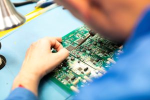
As our reliance on sophisticated electronics continues to grow, the importance of securing the reliability and effectiveness of Printed Circuit Board Assemblies (PCBAs) escalates. A pivotal element in this challenge is addressing Electromagnetic Interference (EMI) while simultaneously achieving Electromagnetic Compatibility (EMC). This blog delves into the complexities of these issues, discussing the challenges encountered during PCB assembly and sharing expert techniques to alleviate these dilemmas.
Understanding EMI and EMC: The Basics
EMI is an unwelcome force that interferes with the optimal performance of electronic circuits. EMC, by contrast, refers to a circuit’s ability to operate harmoniously within its environment, without causing or succumbing to interference. The need for EMC is accentuated by the increased complexity, density and diversity of electrical and electronic components and circuits.
EMI and EMC Challenges in PCB Assembly
As electronics have become more sophisticated, the challenges around maintaining Electromagnetic Compatibility (EMC) and mitigating Electromagnetic Interference (EMI) have intensified. Particularly in PCB assembly, these challenges can compromise both the functionality and reliability of the final product.
- Signal Integrity: Modern PCBAs often incorporate intricate circuit designs to meet higher performance criteria. Ensuring signal integrity in such complex set-ups is an arduous task, especially when a board is susceptible to numerous sources of EMI.
- Component Density: With technological advancements, components have significantly shrunk in size, leading to higher densities on PCBAs. While this miniaturisation has many advantages, it does amplify EMC concerns. Close proximity of components can lead to crosstalk, noise and other forms of interference that compromise the board’s functionality.
- Harmonics and Noise: Increasingly, PCBAs incorporate high-frequency components to enhance performance. While these deliver benefits, they also introduce harmonics and noise into the system. Such undesired frequencies can result in both internal and external EMI issues, affecting not only the PCBA itself but also neighbouring electronic systems.
- Grounding Challenges: Efficient grounding schemes are crucial for ensuring EMC and minimising EMI, but many PCBAs suffer from poor grounding design. This often results in ‘ground loops’, a major source of system noise that can degrade performance.
By recognising and understanding these challenges, electronics manufacturers can take proactive steps to mitigate them. Techniques like strategic component placement, improved grounding schemes and the use of EMI shielding can significantly reduce these issues, ensuring that the end product is both reliable and effective.

Strategies for Overcoming EMI and EMC Challenges in PCB Assembly
Navigating the complex landscape of EMI and EMC issues in PCB assembly calls for a multifaceted approach. A comprehensive understanding of the challenges is only half the battle; implementing effective solutions is equally crucial. Here are some techniques and best practices to tackle these challenges head-on:
- Strategic Component Placement: The initial layout stage is critical for mitigating EMI and achieving EMC. Designers should place critical components first and minimise the length of high-speed traces to reduce the risk of interference. Additionally, keeping analog and digital components separate can also help minimise crosstalk.
- Optimised Grounding Schemes: A robust grounding scheme is foundational to achieving EMC. Designers should aim to minimise ground loops and utilise a ground plane for more efficient current returns, thus reducing system noise.
- Utilising Shielding Techniques: EMI shielding, such as metallic enclosures or foil shields, can be employed around sensitive components. This helps to contain electromagnetic fields and reduces the potential for interference.
- Proper Routing and Trace Geometry: The way traces are routed on a PCB can significantly impact its EMC performance. Designers should aim for short, direct traces and avoid using 90-degree angles, as these can act as antennas, radiating EMI.
- Layer Stacking: Modern multi-layer PCB designs offer an opportunity to sandwich signal layers between ground planes. This reduces both inductance and radiation, aiding in EMC compliance.
- Filtering: Employing filters at I/O ports can help minimise high-frequency noise entering or leaving the PCBA, thus aiding in the suppression of EMI.
- Regular Testing: It’s essential to conduct regular EMC tests during the design and manufacturing stages. These tests provide invaluable data on the board’s performance and highlight areas for improvement.
By employing these strategies, manufacturers can significantly improve the EMC performance of their PCBAs while minimising the impact of EMI. While it may require an upfront investment in time and resources, the payoff comes in the form of reliable, high-performance electronic products, particularly important for critical-to-life applications.
Conclusion and The Road Ahead
As technological advancements continue, the challenges related to EMC and EMI will inevitably evolve. Yet, by staying up-to-date with current techniques and best practices, these challenges can be converted into opportunities for innovation.
Take the Next Step
In need of an electronics manufacturer committed to quality and reliability? Explore the services offered by MPE Electronics. Consider us as your next supplier for PCB assemblies that not only meet but exceed industry standards.
MPE Electronics:
MPE Electronics is an established and experienced contract electronics manufacturer specialising in PCB assemblies and full box build assembly for a wide range of commercial and industrial businesses.
To find out how MPE Electronics’ PCB manufacturing and assembly services can benefit your business, contact our expert and friendly team on +44 (0)1825 764822 or enquiries@mpe-electronics.co.uk.

