

Modern PCB design is not just about making boards smaller, faster or more complex. It is about ensuring those designs can be assembled, inspected, tested and manufactured reliably once they reach production.
That distinction matters.
Across the electronics industry, product development is being shaped by miniaturisation, AI-enabled systems, higher data rates, flexible form factors, sustainability targets and ongoing supply-chain pressure. These trends are changing what engineers can design, but they are also changing what contract electronics manufacturers need to manage during PCB assembly.
For OEMs, product designers and procurement teams, the future of PCB design is therefore closely linked to manufacturability. A design may perform well in simulation, but if it creates soldering challenges, inspection limitations, component availability issues or unnecessary rework, it can still cause delays once production begins.
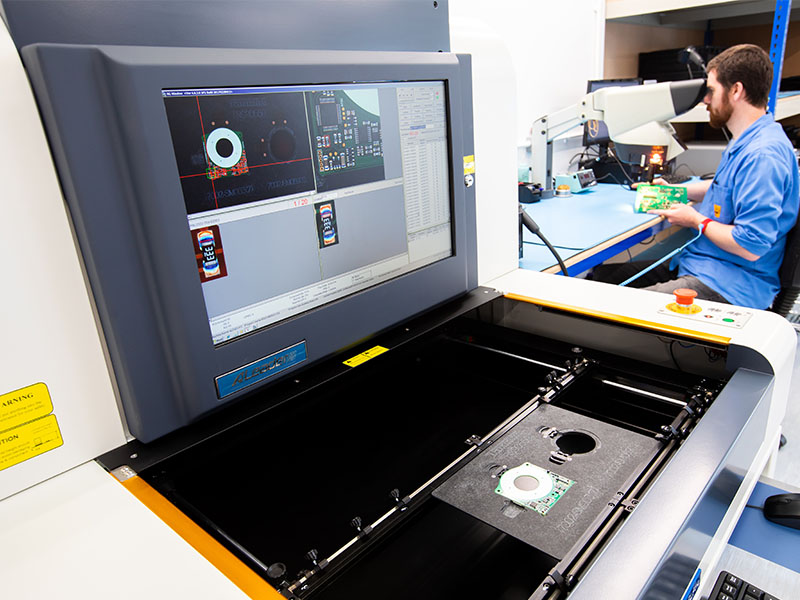
At MPE Electronics, we do not manufacture bare printed circuit boards. We assemble, inspect and test PCB assemblies using approved suppliers, with a focus on quality, traceability and reliability. That gives us a practical view of PCB design trends from the assembly floor: not just what the technology enables, but what it means when a board has to be built consistently.
New Technologies Transforming PCB Design
The electronics industry is seeing renewed momentum, but the next 12 months will be defined as much by constraints as by growth.
AI-driven applications are reshaping demand across the sector. Nowhere is this more evident than in memory products. Strong investment in AI infrastructure continues to pull manufacturing capacity towards high-margin, AI-optimised memory, leading to sustained price increases and tighter availability across mainstream DRAM and NAND.
For many OEMs and system integrators, this means higher costs, longer lead times and a greater need for forward planning, particularly in industrial, embedded and automotive applications where redesign is not always straightforward.
At the same time, AI is driving higher memory content and performance requirements across a growing range of products, from edge devices to industrial systems. More intelligence at the product level means more complex PCB assemblies, tighter layouts, greater thermal demands and increased pressure on component sourcing.
Growth is present in the electronics market, but navigating it effectively requires early engagement, flexible sourcing strategies and close supplier relationships.
AI-Enhanced PCB Design and Predictive Engineering
AI in PCB design is one of the most discussed trends in electronics engineering. AI-assisted tools can help with layout optimisation, routing, design rule checking and simulation-led decision-making. Used well, they can reduce manual design time and identify potential performance issues earlier.
However, the real value of AI PCB design is not simply faster layout generation. It is better decision-making before a design reaches production.
Intelligent Layout, Routing and Rule Checking
As PCB assemblies become denser, small design decisions have a larger impact on assembly quality.
Component spacing, pad geometry, test point access, thermal reliefs and routing choices can all affect soldering, inspection and rework. AI-assisted design tools can help flag potential issues earlier, but they do not replace the need for practical manufacturing input.
For example, an automated layout may achieve electrical performance targets while still creating avoidable production challenges. Components may be positioned too close for effective inspection, test points may be difficult to access, or thermal mass may vary significantly across the board.
These are not theoretical concerns. They directly influence production yield, rework time and long-term reliability.
AI-Driven Manufacturability Analysis
One of the strongest opportunities for AI in PCB design is predictive manufacturability analysis.
If design tools can identify assembly risks before a prototype is built, engineers can reduce the number of design iterations and avoid preventable delays. This is especially important for high-reliability applications, where late changes can affect cost, compliance and launch schedules.
From an assembly perspective, AI-supported design checks should help identify issues such as:
- Inadequate spacing around components
- Poor access for inspection or testing
- Footprints that do not match specified parts
- Thermal imbalance across solder joints
- High-risk via placement
- Component choices with limited availability
These checks are most useful when combined with input from the assembly partner. At MPE Electronics, we regularly support customers by reviewing practical build considerations before production begins, helping reduce rework and improve the transition from prototype to production.
HDI PCB Design and the Manufacturing Impact of Higher Density
High-density interconnect, or HDI PCB design, continues to support the move towards smaller, lighter and more capable electronic products.
HDI designs typically use finer tracks, smaller vias, tighter spacing and higher layer counts. This allows more functionality to be placed into a smaller footprint, which is valuable in medical devices, instrumentation, communications equipment, industrial controls and compact embedded systems.
However, higher density also reduces manufacturing margin.
Smaller Features Require Greater Process Control
As component density increases, assembly becomes more sensitive to solder paste control, placement accuracy, thermal profiling and inspection access.
A small footprint error, incorrect pad size or unsuitable soldering condition can have a disproportionate effect on reliability. This is why PCB design trends cannot be assessed in isolation from the assembly process.
Designers should consider not only whether a board can be routed, but whether it can be assembled repeatedly and inspected effectively.
Ground Planes, Thermal Reliefs and Soldering Reliability
Large copper areas and ground planes are common in modern PCB design. They support electrical performance and thermal management, but they can also act as heat sinks during soldering.
This can make it harder to achieve reliable solder joints, particularly where grounded pads connect directly to large copper planes. In production, this may require additional process controls such as higher soldering iron temperatures, larger iron tips, local preheating or additional flux to improve heat transfer.
Even then, care must be taken. Excessive heat can burn flux, damage components or lift PCB traces.
Designers can reduce this risk by using thermal reliefs where appropriate. These spoke-like connections between pads and copper planes help control heat transfer and improve solderability without compromising the design intent.
This is a good example of where design for manufacture matters. A small layout decision can affect solder joint quality, rework risk and production efficiency.
Flexible and Rigid-Flex PCB Design
Flexible PCB design and rigid-flex PCB design are increasingly important as products become smaller, lighter and more mechanically integrated.
Rigid-flex designs can reduce connectors, cables and interconnects, helping to lower weight and improve reliability in compact assemblies. They are particularly relevant in automotive electronics, medical technology, wearables, aerospace systems and portable industrial equipment.
However, flexible and rigid-flex designs introduce new assembly considerations.
Reducing Interconnects Without Increasing Production Risk
Fewer connectors can mean fewer mechanical failure points, but rigid-flex assemblies require careful planning.
Flexible areas need to be handled correctly during assembly. Component placement must account for bend areas, strain points and support requirements. If components are placed on unsupported flexible regions, assembly accuracy and long-term reliability may be affected.
Where devices are mounted on flexi-rigid assemblies, it is often good practice to provide rigid support beneath the component area. This can improve panelisation, help maintain positional accuracy and reduce reliance on custom jigs during production.
Via Placement and Surface Mount Pads
Designers should also avoid placing vias directly in surface mount pads unless the design has been specifically engineered for that approach.
During soldering, solder can be drawn down through the via, reducing the solder volume at the joint. This can create dry joints and increase rework requirements.
As rigid-flex and flexible PCB designs become more common, early communication between the design team and assembly partner becomes essential. The objective is not just to create a compact design, but to ensure it can be assembled without introducing unnecessary handling, soldering or inspection risk.
High-Frequency PCB Design and Real-World Assembly Performance
High-frequency PCB design is being driven by 5G, RF communications, radar, industrial connectivity, high-speed data systems and advanced sensing applications.
These applications often require controlled impedance, low-loss materials, careful layer stack-ups and strict routing discipline. Signal integrity is central to performance, particularly in super high frequency and extremely high frequency applications.
However, high-frequency performance is not determined by layout alone.
Assembly Quality Affects Electrical Performance
Poor solder joints, inconsistent grounding, thermal variation and manufacturing inconsistencies can all affect high-frequency behaviour.
For engineers, this means assembly quality should be considered alongside simulation and material selection. The board must not only meet electrical requirements on paper; it must maintain those characteristics across production builds.
High-frequency assemblies may also require more careful inspection and test planning. If components are densely packed or shielding restricts visibility, design teams should consider how quality checks will be carried out during production.
Materials and Thermal Behaviour
Advanced PCB materials often behave differently during assembly compared with standard FR4. Low-loss dielectrics, high-speed laminates and specialist substrates may require careful consideration of thermal profiles, moisture sensitivity and handling requirements.
This matters because thermal behaviour affects soldering consistency and component reliability.
As high-frequency PCB requirements become more common, practical assembly input becomes increasingly valuable during the design stage.
Additive Manufacturing and 3D PCB Architecture
Additive manufacturing is often discussed as part of the future of PCB design.
In PCB development, additive manufacturing refers to building conductive pathways, substrates or structural elements layer by layer rather than relying only on traditional subtractive copper etching methods. It opens possibilities for 3D PCB design, embedded pathways, rapid prototyping and more complex product geometries.
This has clear potential, particularly for early-stage development and specialist applications where conventional board layouts are restrictive.
However, from a production perspective, additive manufacturing still needs to be assessed through the lens of reliability, repeatability, inspection and test.
Prototyping Potential and Production Reality
Additive methods can support rapid design iteration and complex geometries, but production teams still need to understand:
- Material consistency
- Solderability
- Long-term reliability
- Inspection access
- Repairability
- Compatibility with established assembly processes
For regulated or safety-critical applications, new production methods must be validated carefully before being adopted at scale.
The opportunity is significant, but the same principle applies: innovation must be balanced with manufacturability.
Embedded Components and System-in-Board Integration
Another important PCB trend is the integration of components within the board structure itself.
Embedded passives, sensors or controllers can reduce surface component count, save space and improve electrical performance. This can support miniaturisation and improve protection for sensitive components.
However, embedded component strategies also change how boards are assembled, inspected and repaired.
Reliability, Heat and Test Access
When components are hidden within the PCB structure, inspection becomes more complex. Testing strategies must be planned early, because visual inspection alone may not be sufficient.
Thermal management is also important. Embedded components can generate heat within the board, so designers need to consider how that heat will be dissipated across the assembly.
For procurement and operations teams, embedded components may also affect sourcing flexibility and rework options. If an embedded part becomes obsolete or unavailable, redesign can be more difficult than with surface-mounted alternatives.
This reinforces the need for early Bill of Materials (BOM) review and lifecycle planning.
Digital Twins, Simulation and Virtual Prototyping
Simulation-first workflows are becoming more widely used in PCB design. Digital twins and virtual prototypes allow engineers to test electrical, thermal and mechanical performance before physical prototypes are built.
This can reduce development time and identify design risks earlier.
However, simulation must be supported by practical manufacturing knowledge.
A virtual model may show that a layout performs correctly, but it may not always account for production realities such as soldering access, panelisation, component variation, inspection constraints or supply-chain availability.
For the best results, simulation should be used alongside design for manufacture review. This helps ensure the design is not only technically sound, but practical to build.
Hardware-Level Security and Connected Devices
As more products become connected, PCB design is increasingly being influenced by hardware security requirements.
Secure routing, tamper-evident board structures and protected interfaces are becoming more relevant in access control, industrial systems, defence electronics and connected infrastructure.
For assembly teams, these requirements can introduce additional process controls. Sensitive assemblies may require tighter documentation, traceability and inspection procedures.
MPE Electronics works with customers in sectors where reliability, compliance and traceability are critical. In these environments, secure and controlled assembly processes are not optional extras; they are part of reducing product and supply-chain risk.
Sustainability and Efficient PCB Design
Sustainability in PCB design is often associated with materials, recyclability and energy efficiency. These are important, but they are not the whole picture.
A design that creates avoidable scrap, rework or inefficient production also has a sustainability impact.
Efficient PCB design should therefore consider manufacturability from the outset.
Designing to Reduce Waste and Rework
Production waste can be reduced through:
- Accurate documentation
- Suitable component selection
- Efficient panelisation
- Good solderability
- Clear test access
- Reduced rework risk
- Early identification of obsolete or difficult-to-source parts
Design for manufacture supports sustainability because it helps prevent unnecessary delays, rejected assemblies and repeated prototype cycles.
Panelisation and Board Separation
Panelisation is one of the practical areas where design decisions affect cost, efficiency and risk.
Where possible, rectangular or square PCB designs can allow V-scoring, which is fast and cost-effective for straight-edged boards. This can support efficient production, particularly where volumes are higher and board geometry is simple.
More complex shapes may require routing. Routing offers better edge quality and greater flexibility for curved or irregular outlines, but it is generally more expensive and may increase production time.
Designers should also consider where components are placed in relation to board edges. Edge-mounted components or fragile areas can be damaged during depanelisation if the board has not been planned carefully.
Considering panelisation early can reduce handling risk, improve throughput and support more efficient manufacturing.
What Designers Can Learn from the Assembly Floor
Many PCB design trend articles focus on advanced technologies. In production, however, some of the most common delays still come from avoidable issues in documentation, component selection and design handover.
At MPE Electronics, we see how incomplete or inconsistent information can slow quotation, procurement and production.
Common issues include:
- Missing manufacturer part numbers
- Incomplete or incorrect BOM data
- Obsolete components in older designs
- Incorrect component descriptions
- Footprints that do not match the specified part
- Missing circuit references
- Missing drawings or build instructions
- Inconsistent file formats between customers
These issues require clarification before production can proceed. MPE queries uncertainties rather than making assumptions, because assumptions introduce risk.
For designers, the lesson is straightforward: the quality of the manufacturing handover is part of the design.
Practical Design Tips for Smoother PCB Assembly
To reduce production risk, designers should:
- Provide full manufacturer part numbers on the BOM
- Include circuit references and quantities for every fitted component
- Ensure footprints match the specified components
- Avoid obsolete, long-lead-time or single-source parts where possible
- Provide all relevant drawings, build guides and assembly instructions
- Consider component availability and cost during design
- Use surface mount components where appropriate to improve production efficiency
- Plan panelisation and board separation early
- Avoid vias in surface mount pads unless specifically designed for that process
- Use thermal reliefs where suitable to improve solderability
These details may seem basic compared with AI, HDI or additive manufacturing, but they often have the greatest impact on whether a project moves smoothly from design to production.
What PCB Design Trends Mean for Procurement Teams
PCB design trends do not only affect engineers. They also affect procurement, operations and supply-chain planning.
As designs become more advanced, the choice of components, materials and manufacturing processes becomes more strategic.
AI-driven demand is already placing pressure on memory products, with higher costs and longer lead times affecting mainstream DRAM and NAND. At the same time, advanced designs may depend on specialist laminates, smaller packages, rigid-flex constructions or tightly specified components.
Procurement teams should therefore be involved early, particularly where redesign would be difficult later.
Key considerations include:
- Component availability
- Approved alternatives
- Obsolescence risk
- Lead times
- Supplier reliability
- Minimum order quantities
- Documentation quality
- Test and inspection requirements
Strong collaboration between design, procurement and manufacturing teams helps reduce risk before it becomes a production issue.
Preparing for the Future of PCB Design
The future of PCB design will be shaped by AI, HDI, flexible electronics, high-frequency applications, additive manufacturing, embedded components and sustainability requirements.
But the most successful projects will not be defined by technology alone.
They will be defined by how well those technologies are translated into reliable, manufacturable PCB assemblies.
For engineers, this means considering assembly, inspection, testing and sourcing earlier in the design process. For procurement teams, it means understanding how design decisions influence lead times, component risk and production continuity. For OEMs, it means choosing manufacturing partners who can support the transition from prototype to production with clear communication and controlled processes.
At MPE Electronics, we support customers with PCB assembly, prototyping and full product assembly for high-reliability applications. Our production team is trained in component recognition, ESD best practice and IPC-A-610, with selected staff also trained to IPC 7711/21. Every assembly is inspected individually, with traceability and quality control built into the process.
PCB design trends will continue to evolve. The priority is ensuring that innovation does not create avoidable risk when the board reaches production.
To discuss your PCB assembly or box-build requirements, contact MPE Electronics on +44 (0)1825 764822 or email enquiries@mpe-electronics.co.uk.
