

A detailed PCB assembly drawing serves as a crucial tool to minimise any misinterpretation, manufacturing or assembly errors, quality and compliance issues, as well as cost and time overruns. In this blog post, you will learn about the two principal types of drawings that contribute to the development of a Printed Circuit Board Assembly (PCBA), the level of detail required and how your contract electronics manufacturer (CEM) can support you throughout the process.
Fabrication and assembly process overview
Typically, there are two phases in the fabrication of a PCB assembly: the first involves laminating layers of dielectric material with copper foils, forming interconnects, then etching and applying a solder mask; the second, the assembly phase, involves components being soldered onto the PCB, inspected, and tested for functionality and quality assurance. In order for these two phases to seamlessly interconnect, highly detailed drawings are required. These drawings contain all the specifications, notes, instructions and more, which enable the contract manufacturer to produce the final assembly. Separate drawings are required to define how the raw printed circuit board itself is to be built and how the components are to be attached to it. Careful selection of design tools can streamline the drawing process. Advanced software such as AutoCAD and Altium Draftsman automate PCB design, reducing the risk of omitting crucial information needed by the manufacturer.
PCB fabrication drawing
The drawing elements required to produce the raw board itself will depend on the intended application, but generally the PCB fabrication drawing includes the board outline, part shapes with ‘reference designators’ (i.e. the location of where the components are to be placed) and mechanical parts with their mounting hardware (e.g. a cable connector and screws). It is worth noting that some design tools may not include this feature automatically and will need to be manually added to the drawing. Dimensions and scale, as well as drawing version number and approval signature must be included in the drawing details. Notes or instructions as to how the board will be manufactured, including references to industry standards and specifications, must also be clearly indicated. The items listed above are what a basic ‘fab drawing’ will include, however including the more specific drawing elements listed below will ensure clear communication with the board manufacturer:
- Drill hole legend/table, showing hole sizes, locations, and purposes (such as component mounting or vias)
- Layer stack up table, indicating material type, thickness, layer stack up configuration, Dielectric Constant (Dk) and copper weights
- Details of the solder mask layer, including colour, thickness and openings for exposed copper areas
- Specifications for copper traces, including widths, spacings and clearances, as well as details of copper planes
- Surface finish requirements
- Tolerances for etching and plating, and the board itself
- Side and back views of the board outline to showcase any curves or circular details
The next phase is to create the PCB assembly drawing. 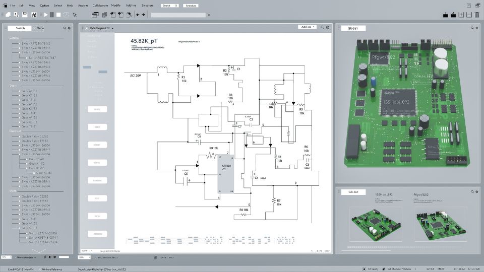
PCB assembly drawing
In its most basic form, the PCB assembly drawing must provide enough detail to instruct your electronics manufacturer as to how the components will be attached to the fabricated PCBs. Specifically, the following information is required:
- Component placement instructions indicating where each component should be placed on the PCB, often including reference designators and polarity markings
- Clear indications of the orientation of components to ensure they are correctly aligned on the PCB
- Bill of Materials (BOM) listing all components required for assembly, including part numbers, descriptions, quantities and vendor information
- Specifications for soldering processes, including soldering temperatures, solder type and any special instructions for specific components
- Assembly notes, including any additional instructions or notes relevant to the assembly process, such as special handling requirements or test procedures.
- Location and labelling of test points or pads for performing functional tests or quality assurance checks
The PCB assembly drawing is pivotal in guiding the assembly process, ensuring accurate component placement and soldering alignment with design specifications. Implementing practices such as enlarging specific areas of the drawing and incorporating ‘callouts’ or text boxes, enhances clarity, accuracy and communication of precise details. This supports effective quality inspection processes, facilitating thorough scrutiny and adherence to standards. Looking for a CEM partner to assemble your PCBA for your next product? Learn more about our PCB assembly service here
Collaborating with your contract manufacturer
As highlighted earlier, PCB and PCB assembly drawings play a pivotal role in conveying your specific requirements to your contract manufacturing partner. However, effective communication should commence prior to the drawing phase. A collaborative CEM acts as a valuable partner throughout your PCB assembly development journey. Seasoned PCB assembly partners like MPE offer expertise to help you select high-quality parts and materials at competitive prices. They provide layout recommendations that optimise both operational efficiency and practical assembly considerations. Engaging with your CEM early allows them to outline specific requirements before PCB assembly drawing begins, streamlining the process and minimising iterations. Once completed, PCB assembly drawings can be shared in various formats to accommodate stakeholders’ needs. Formats such as PDFs and Gerber files, and cloud-based platforms, such as Dropbox, facilitate seamless communication between you and your CEM, ensuring clarity and alignment before manufacturing and assembly commence.
Detail and precision are key
The PCB fabrication and PCB assembly drawings should be created with enough detail to ensure that anyone anywhere at any time can interpret them correctly. The intended application for the PCB assembly will determine the level of detail and exact drawing elements required, but early communication with your selected CEM is important when it comes to successfully minimising the risks associated with PCB assembly production. MPE Electronics is an established and experienced contract electronics manufacturer specialising in PCB assemblies and full box build assembly for a wide range of commercial and industrial businesses. To find out how MPE Electronics’ PCB manufacturing and assembly services can benefit your business, contact our expert and friendly team on +44 (0)1825 764822 or enquiries@mpe-electronics.co.uk.
