
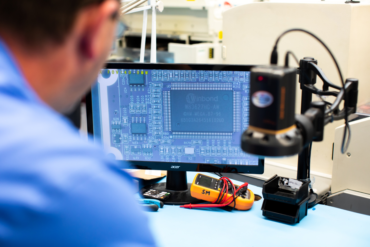
PCB inspection is essential wherever electronic assemblies must perform reliably throughout their intended service life. A solder joint may appear small, but its quality can affect electrical performance, mechanical strength and the reliability of the finished product. For OEMs, engineers and procurement teams, effective inspection is therefore not simply a final check. It is a controlled process that helps prevent rework, production delays and failures in the field.
What Is PCB Inspection?
Before considering individual defects, it is important to understand what inspection covers.
PCB inspection is the examination of an assembled printed circuit board to confirm that components, solder joints and workmanship meet the specified requirements. It can take place at several stages of the PCB assembly process, rather than being limited to the end of production.
The inspection process may verify:
- Component presence, type, value and orientation
- Component positioning and alignment
- Solder joint quality
- Polarity markings
- Visible damage or contamination
- Conformity with drawings and customer specifications
- Workmanship against relevant IPC standards
Inspection should form part of a wider quality assurance system that includes controlled materials, documented processes, trained personnel and product traceability. Finding a defect is useful, but understanding why it occurred and preventing its recurrence provides greater long-term value.
Why PCB Inspection Matters in PCB Assembly
That wider process matters because a defect can create consequences well beyond the assembly line.
A poor solder joint may initially pass an electrical check but fail later through vibration, thermal cycling or repeated use. Incorrectly positioned components can also affect performance, create intermittent faults or prevent the assembly from functioning altogether.
For products used in medical, industrial or safety-critical environments, those risks require particularly careful control. Reliability is not optional when an electronic assembly supports essential equipment or operates in demanding conditions.
Effective PCB assembly quality control helps manufacturers identify problems before assemblies progress into box-build, final testing or customer delivery. This reduces the cost and disruption associated with dismantling finished products to investigate faults.
It also protects:
- Production schedules and delivery commitments
- Product performance and service life
- Warranty costs and customer satisfaction
- Compliance and traceability records
- The OEM’s reputation in their target market
At MPE Electronics, every PCB assembly is individually inspected rather than relying on batch sampling alone. This allows issues to be identified at assembly level and supports clear traceability throughout production.
Common PCB Soldering Defects
To control these risks effectively, manufacturers must recognise the defects most likely to affect an assembly.
Cold solder joints
A cold solder joint can occur when the solder does not melt or flow correctly. The resulting connection may appear dull, irregular or poorly bonded. Although it may provide initial electrical continuity, it can be mechanically weak and vulnerable to intermittent failure.
Solder bridges
A solder bridge forms when solder unintentionally connects two adjacent pads, component leads or tracks. This can cause a short circuit and prevent the assembly from operating correctly. Fine-pitch components require especially close process control because spacing is limited.
Insufficient solder
Too little solder can leave a joint without adequate electrical or mechanical strength. The cause may relate to solder paste deposition, component placement, process settings or manual soldering technique.
Excess solder
Excessive solder can obscure the joint, make inspection more difficult or create unintended connections. More solder does not necessarily produce a stronger joint. The correct quantity and joint profile are more important.
Voids
Voids are pockets within a solder joint where the expected solder material is absent. Their significance depends on their size, position, component type and acceptance criteria. Some joints cannot be fully assessed through visual inspection alone.
Lifted pads
A lifted pad separates from the PCB surface, often because of excessive heat, mechanical force or repeated rework. This can damage the electrical connection and may make repair more complex.
Component misalignment
A component may be present but positioned incorrectly on its pads. Misalignment can reduce the soldered contact area or create inconsistent joint formation. Severe movement can cause open circuits or bridging.
Tombstoning
Tombstoning occurs when one end of a small surface-mount component lifts during reflow. The component stands partially upright, leaving one termination disconnected. Uneven heating, pad design or solder wetting can contribute to the defect.
These problems demonstrate why PCB soldering cannot be judged by appearance alone. Defect analysis should consider the process, design, materials and acceptance requirements together.
PCB Inspection Methods for Identifying Soldering Defects
As defects vary in type and location, no single inspection method is suitable for every assembly.
Visual inspection
Visual inspection is used to assess accessible components and solder joints. A trained inspector can identify issues such as missing components, incorrect orientation, poor solder profiles, contamination and visible damage.
Magnification may be used where component size or spacing makes unaided inspection unsuitable. The inspection criteria should be defined by the assembly specification and applicable workmanship standards.
Automated optical inspection
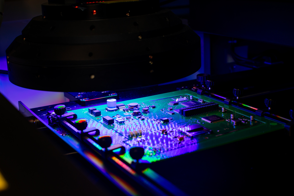
Automated optical inspection, or AOI, uses programmed imaging systems to check assemblies against defined criteria. It can identify component presence, alignment, polarity and certain visible soldering defects.
AOI supports consistency, particularly across assemblies containing many surface-mount components. However, it should be programmed and reviewed by knowledgeable personnel. Automated inspection supports process control; it does not remove the need for engineering judgement.
X-ray inspection
X-ray inspection can reveal features that are hidden beneath components or within solder joints. It may be appropriate for assemblies containing bottom-terminated components where connections cannot be viewed directly.
The inspection method should be selected according to component package, product risk and customer requirements. Not every assembly needs every inspection technology.
Functional testing
Functional testing checks whether an assembly or completed product performs as intended. It can identify problems that visual methods may not detect, including electrical faults, incorrect behaviour or failures under specified operating conditions.
Where required, inspection can be supported by environmental and electronics testing. The appropriate test strategy should be agreed early, based on the application and its reliability requirements.
How Soldering Defects Affect Product Quality and Reliability
Inspection methods only provide value when they are connected to the product’s real operating conditions.
Consider a control board used within industrial equipment. A marginal solder joint may work during initial power-up and appear acceptable during a basic test. Once installed, however, repeated temperature changes and vibration could weaken the connection until an intermittent fault develops.
The result may be unplanned equipment downtime, a service visit and a difficult fault investigation. If the failure is intermittent, identifying the root cause can take longer than replacing the assembly itself.
This illustrates the difference between basic defect detection and effective quality control in electronics manufacturing. The objective is not simply to find visibly poor workmanship. It is to reduce the probability of defects entering the product and affecting performance later.
Robust PCB quality control also provides useful feedback. If the same type of defect appears repeatedly, the manufacturer can investigate potential causes such as stencil design, paste application, placement accuracy, thermal profiling or component condition.
Preventing PCB Soldering Defects Through Effective Quality Control
For that reason, prevention should begin before the first assembly enters production.
Clear manufacturing data, suitable component footprints and accessible inspection points can all improve manufacturability. Early design review can identify issues that might otherwise lead to inconsistent solder joints, difficult inspection or unnecessary rework.
Effective electronics manufacturing quality control should include:
- Review of drawings, bills of materials and manufacturing information
- Procurement through approved suppliers
- Controlled component storage and handling
- Documented surface-mount and through-hole processes
- Appropriate soldering profiles and equipment settings
- Inspection against the agreed specification
- Traceability of materials and production activity
- Investigation and recording of non-conformances
Recognised standards provide a common reference point. IPC-A-610 defines acceptance requirements for electronic assemblies, while IPC J-STD-001 addresses requirements for soldered electrical and electronic assemblies. The relevant class and acceptance criteria must reflect the product specification and intended application.
MPE supports both surface-mount technology and through-hole assembly, with inspection and traceability built into the manufacturing process. This provides a controlled route from component procurement through to completed assembly.
Choosing a PCB Assembly Partner with Robust Inspection Processes
Once the required controls are understood, the next question is whether a manufacturing partner can apply them consistently.
Engineers and procurement teams should ask how inspection fits into the supplier’s complete production process. A list of equipment is not enough. The supplier should be able to explain when checks occur, how results are recorded and what happens when an issue is identified.
Useful questions include:
- Is every assembly inspected or only a sample from each batch?
- Which IPC standards and customer specifications are followed?
- How are materials and production stages traced?
- When is AOI used and how are findings reviewed?
- How are defects recorded and investigated?
- Can the supplier support prototypes and changing volumes?
- How are design or manufacturing concerns communicated?
A capable partner should also support the wider product journey. MPE provides turnkey PCB assembly and full box-build services, helping customers reduce supplier handovers and maintain control as products move from assembly into final integration.
This collaborative approach is especially valuable during new product introduction. Identifying risks before production begins is usually more efficient than correcting them after components have been placed and soldered.
Frequently Asked Questions
What is PCB inspection?
PCB inspection is the examination of an assembled circuit board to check component placement, solder joints, workmanship and conformity with the relevant specification.
Why is PCB inspection important?
It helps identify defects before products reach later manufacturing stages or enter service. This reduces rework, delays and the risk of field failures.
What are the most common PCB soldering defects?
Common defects include cold joints, solder bridges, insufficient solder, excess solder, voids, lifted pads, misaligned components and tombstoning.
How are soldering defects identified?
Methods can include visual inspection, magnified inspection, AOI, X-ray inspection and functional testing. The correct combination depends on the assembly and its application.
What is the standard for PCB inspection?
IPC-A-610 is widely used for electronic assembly acceptance. IPC J-STD-001 covers requirements for soldered electrical and electronic assemblies. The applicable requirements should be confirmed for each product.
What are the main PCB testing methods?
Testing approaches can include visual inspection, AOI, X-ray inspection, in-circuit testing, flying-probe testing, functional testing and environmental testing. Not every method is required for every product.
How does PCB inspection improve product reliability?
Inspection identifies workmanship and assembly issues before they can affect the finished product. Combined with controlled processes and defect analysis, it also helps prevent recurring faults.
Reduce Production Risk with Controlled PCB Inspection
PCB inspection should be treated as part of the complete manufacturing process, not as a single check before dispatch. When supported by trained personnel, traceability, appropriate testing and clear acceptance criteria, it protects both product reliability and production efficiency.
MPE Electronics provides flexible PCB assembly and box-build services for low-to-mid volume, high-reliability applications. We inspect every PCB assembly individually and work closely with design, procurement and operations teams to ensure requirements are understood throughout production.
To discuss PCB inspection, assembly requirements or a new product introduction, contact MPE Electronics. Further technical information is also available in our electronics manufacturing guides.
